Scientists measured the displacement cross section of Sulphur atoms in MoS2 at temperatures up to 550◦C using scanning transmission electron microscopy at acceleration voltages of 60 and 90 keV.
At a temperature of 150◦C, the displacement cross section of S atoms increased compared to room temperature, which is due to a thermal activation of phonons which increase the maximum transferred energy (highest amount of energy that an electron from the electron beam can transfer to an atom). At higher temperatures the measured cross section decreases significantly. This occurs due to thermal diffusion.
The number of migration steps µ for the defect taken during one image at a given temperature T is

where Em is the migration energy barrier.
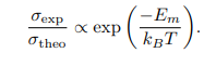
The ratio of the observed and theoretical cross sections which show how the observed defect rate decreases at high temperatures due to the increased migration of vacancies out of the microscope’s field of view.
In study, chemical vapor deposition (CVD) and Scanning Transmission Electron Microscopy were used. Gaussian Distribution was applicable at 60keV. Here CVD is a process used to create very thin, high-quality materials by depositing atoms or molecules layer by layer on a surface.
High temperatures don’t actually reduce or stop the formation of defects caused by the electron beam, they only make the defects difficult to see.
These findings improve understanding of how monolayer MoS₂ responds to electron beams, which is important for its use in electronic devices and for precise material engineering.
Source: https://arxiv.org/html/2411.03200v1
0 comments:
Post a Comment